
How Wall Thickness and Gate Position Affect Conductive PP Resistance Distribution
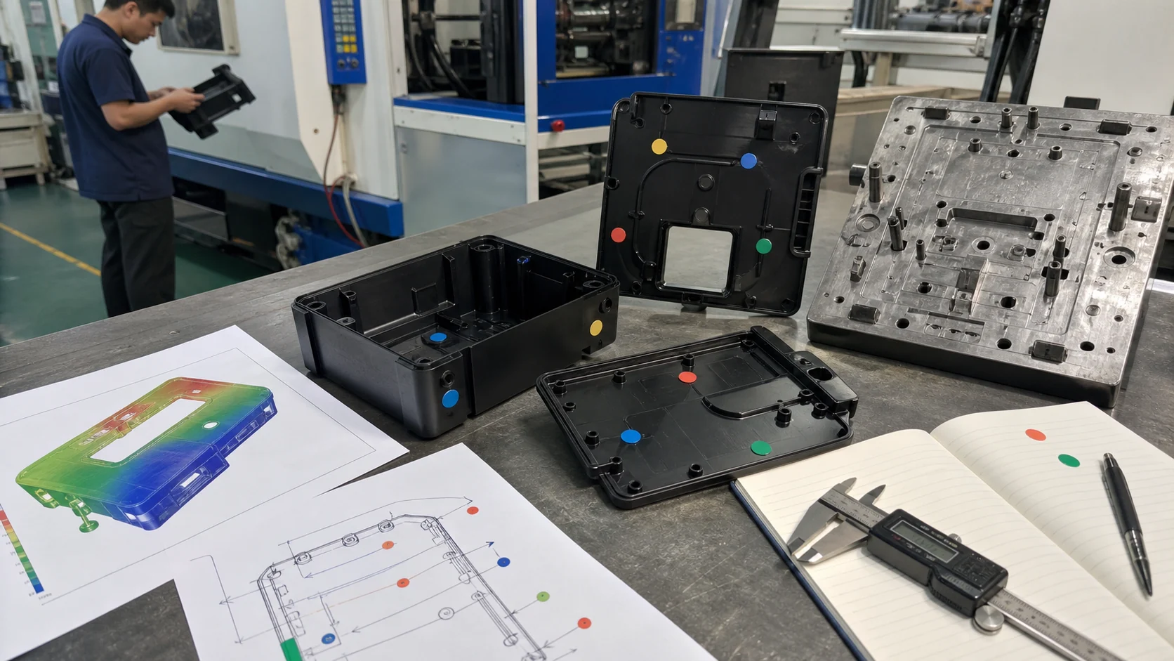
Conductive PP parts can pass resistance testing at one location and fail at another. The material may be the same, but wall thickness, gate position, weld lines and flow direction decide whether ESD performance is uniform on the molded part.
Engineering FAQ
How Wall Thickness and Gate Position Affect Conductive PP Resistance Distribution
Why can the same conductive PP part show different resistance values?
Because injection molding changes filler orientation by flow path, wall thickness, shear, cooling and weld-line formation. A single molded part can therefore have different resistance near the gate, at mid-fill, at the end of fill and around bosses.
Is a pellet resistance value enough for conductive PP qualification?
No. Pellet data is only a starting point. The final ESD performance must be measured on the molded part, at the actual critical surfaces and in the directions relevant to use.
Which wall thickness is safer for conductive PP?
For many conductive PP parts, 1.5-2.0 mm is a practical starting range. Walls below 1.0 mm require very careful gate and process control, while walls above 3.0 mm need attention to skin-core differences.
What should DEYU receive before recommending a conductive PP route?
Send drawings, wall thickness, proposed gate location, ESD target, measurement method, critical surfaces, current failure data and molding conditions. DEYU can then help with material direction, gate review and resistance mapping.
Background / Problem
A recurring challenge in conductive plastics manufacturing is that two parts molded from the same material, in the same mold, can show dramatically different resistivity values depending on where they are measured. Resistance near the gate may sit in a passing range, while the same part can fail at the end of fill, on a thin wall or at a weld line. The difference may reach several orders of magnitude in a single molding cycle.
The root cause is often not only the pellet formulation. It is the part geometry and the way the melt travels through that geometry.
Wall thickness and gate position are two of the most consequential design decisions for conductive plastic parts. They directly determine flow length and pressure distribution, shear rate and filler alignment, cooling rate and skin-core structure, and the location and severity of weld lines.
Ignoring these factors creates practical costs: parts pass resistance testing at one point but fail at another, ESD performance varies from batch to batch, scrap rises because parts cannot meet the specification, field failures appear on marginal conductive surfaces, and design or tooling investment is wasted on parts that cannot be molded consistently.
For direct material context, DEYU publishes DGK-PP DD2-3A conductive PP. For broader selection logic, see the conductive PP molded-part selection guide. The grade mentioned in the customer trial as DGK-PP DD4-5 is treated here as an internal trial direction, not as a public product page.
Technical Difficulty: Why Geometry Affects Resistance Distribution
Flow length and pressure drop: the gate-to-end-of-fill gradient
During injection molding, melt pressure is highest at the gate and decreases as the melt travels through the cavity. Near the gate, high pressure and shear can create a dense but strongly oriented filler structure. In the mid-fill area, pressure and shear become more balanced. At the end of fill, lower shear may allow a more random filler network, but packing may also be weaker. Research on conductive molded composites often shows a counterintuitive result: the area closest to the gate is not always the most conductive, because excessive shear can disrupt conductive paths.
Wall thickness: shear rate and cooling effect
| Wall Thickness | Shear Rate | Cooling Rate | Filler Orientation | Resistivity Characteristic |
|---|---|---|---|---|
| Thin (<1.0 mm) | High | Fast | Strongly aligned with flow | High anisotropy; higher surface resistivity |
| Moderate (1.5-2.5 mm) | Moderate | Moderate | Balanced orientation | More uniform resistivity |
| Thick (>3.0 mm) | Low | Slow | Random / less oriented | Lower anisotropy; possible core conductivity |
Wall thickness changes both shear rate during filling and cooling rate after filling. Thin walls create high shear and rapid cooling, which orient fillers in the flow direction and can increase anisotropy. Moderate walls give a more balanced orientation. Thick walls reduce shear but cool slowly, increasing the possibility of a different core structure. In PP/MWCNT nanocomposites, reported resistivity variation inside one molded plate can reach up to five orders of magnitude at low nanotube loading.
Skin-core structure: through-thickness resistivity gradient
| Layer | Formation | Filler Orientation | Resistivity |
|---|---|---|---|
| Skin | Rapid cooling at mold wall | Strongly aligned with flow | Higher surface resistivity |
| Sub-skin | Transition zone | Moderate alignment | Variable |
| Core | Slow cooling in the center | Random or less oriented | Lower resistivity, more conductive |
Injection molded parts form a skin-core structure. The skin cools rapidly against the mold wall and usually has stronger filler alignment. The core cools more slowly and can retain a more random filler network. Surface resistance measurements mostly read the skin layer, so they may not represent through-thickness conductivity. In conductive molded systems, both flow-direction and thickness-direction differences must be considered.
Gate position: flow path and weld-line determinant
Gate position defines the flow path. A single edge gate creates a long flow path and strong filler alignment. A center gate creates radial flow and often shorter paths. Multiple gates reduce flow length but introduce multiple weld lines. Gate placement also decides whether a weld line lands on a critical ESD surface or in a low-risk area.
Weld lines: localized failure point
Weld lines occur where two melt fronts meet. At that interface, fillers can relax, rotate or become depleted, and the conductive network may be interrupted. For surface ESD performance, a weld line is often the most likely localized high-resistance zone, especially around bosses, ribs and windows where flow fronts split and reunite.
Filler orientation: anisotropy driver
Anisotropic fillers such as carbon fiber, CNT and high-structure carbon black align with melt flow. Conductivity along the flow direction can be higher, while transverse and through-thickness conductivity can be lower. Wall thickness and gate position control the degree of alignment because they control shear rate and flow length.
DEYU Material Direction: Design Guidelines for Uniform Resistance
DEYU approaches conductive PP part design through a combined material, mold and validation framework. The goal is not to chase one low pellet value, but to make the final molded part meet the target at every critical surface.
Wall thickness design guidelines
| Design Element | Recommendation | Rationale |
|---|---|---|
| Minimum wall thickness | >=0.8 mm for conductive PP | Below this, high shear can disrupt filler networks |
| Optimal range | 1.5-2.0 mm | Balances flow, shear and cooling for uniform resistivity |
| Maximum wall thickness | <=3.0 mm | Above this, cooling becomes non-uniform and skin-core differences rise |
| Thickness transitions | Gradual, preferably <=3:1 ratio | Abrupt changes create flow disturbance and resistance hotspots |
Gate position design guidelines
| Design Element | Recommendation | Rationale |
|---|---|---|
| Gate location | Place gates in thicker sections | Improves packing and reduces uncontrolled orientation |
| Flow path length | Minimize gate-to-end distance | Shorter paths reduce pressure drop and resistance gradients |
| Gate type | Use fan or film gates for large parts | Reduces local shear and filler damage |
| Multiple gates | Consider when flow length exceeds 150 mm | Shortens flow path, but weld lines must be managed |
| Critical surfaces | Keep weld lines away from ESD contact surfaces | Weld lines are high-risk resistance zones |
Flow path design guidelines
| Design Element | Recommendation | Rationale |
|---|---|---|
| Flow path geometry | Use gentle curves and avoid sharp corners | Sharp corners change shear and filler orientation |
| Flow length | <150 mm for a single gate when possible | Longer paths create stronger resistance gradients |
| Flow balance | Balance all cavities in multi-cavity tools | Unbalanced filling causes cavity-to-cavity resistance variation |
Processing optimization for geometry
| Parameter | Recommended Direction | Why |
|---|---|---|
| Melt temperature | Use upper recommended range for thin walls | Improves flow and reduces excessive shear |
| Injection speed | Moderate for thin walls; lower for thick walls | Balances filling and filler orientation |
| Mold temperature | Higher for thin walls | Reduces skin-core differences |
| Packing pressure | Optimize by wall thickness | Compensates shrinkage without over-orienting fillers |
Reference Product Data: Resistivity Distribution by Geometry
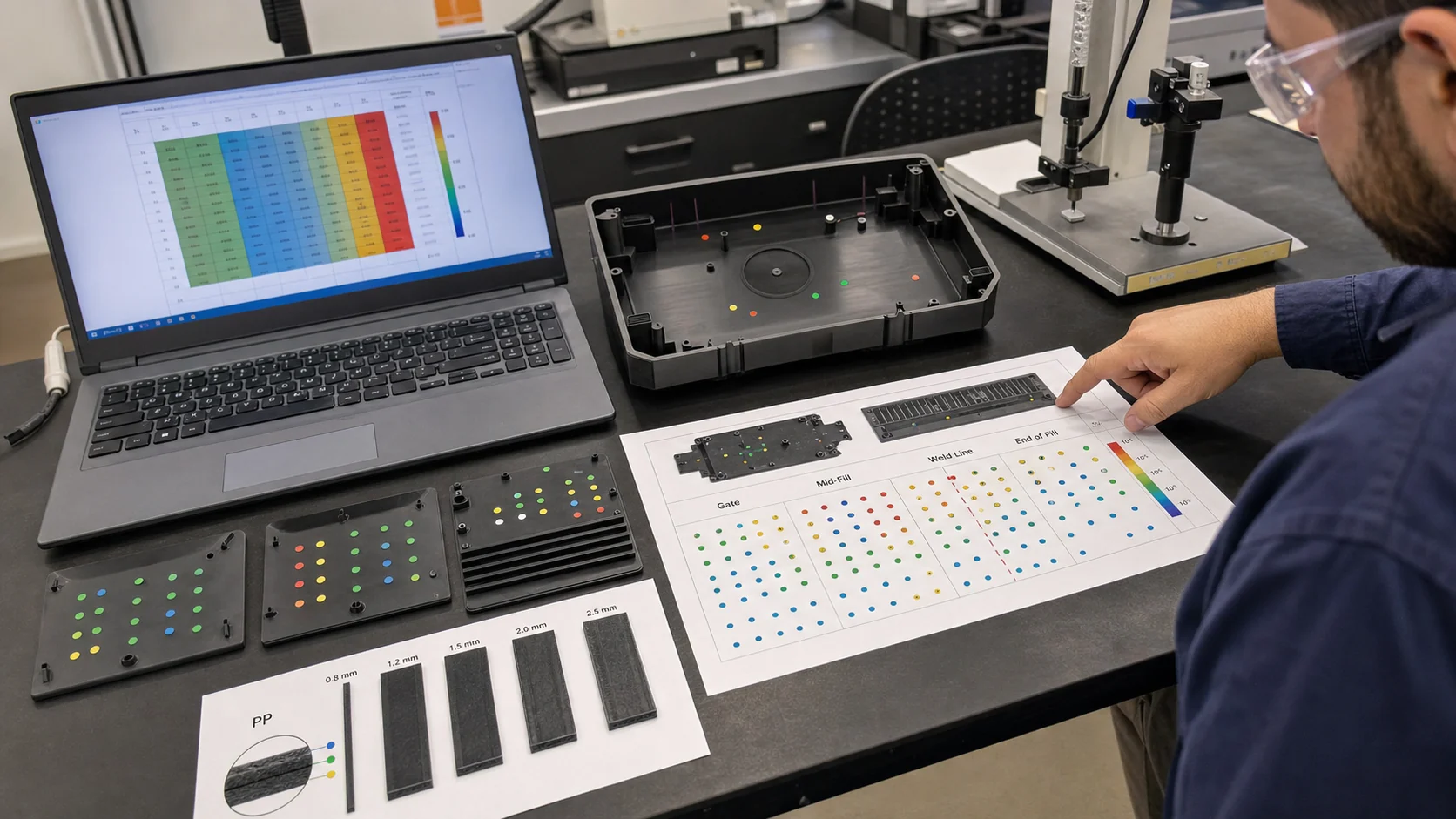
The following reference data shows how wall thickness and gate position may affect resistance distribution for a typical conductive PP trial direction. Values are directional and should be validated on the real part.
| Wall Thickness | Gate Position | Location | Surface Resistivity | Variation | Primary Factor |
|---|---|---|---|---|---|
| 0.8 mm | Edge gate | Near gate | 5 x 10^5 ohm/sq | 1x | High shear |
| 0.8 mm | Edge gate | Mid-fill | 8 x 10^6 ohm/sq | 16x | Filler orientation |
| 0.8 mm | Edge gate | End of fill | 5 x 10^7 ohm/sq | 100x | Low shear and pressure drop |
| 0.8 mm | Edge gate | Weld line | 8 x 10^8 ohm/sq | 1,600x | Filler depletion |
| 1.5 mm | Edge gate | Near gate | 3 x 10^5 ohm/sq | 1x | Moderate shear |
| 1.5 mm | Edge gate | Mid-fill | 6 x 10^6 ohm/sq | 20x | Balanced orientation |
| 1.5 mm | Edge gate | End of fill | 2 x 10^7 ohm/sq | 67x | Moderate pressure drop |
| 1.5 mm | Edge gate | Weld line | 6 x 10^6 ohm/sq | 20x | Partial recovery |
| 2.5 mm | Edge gate | Near gate | 4 x 10^5 ohm/sq | 1x | Lower shear |
| 2.5 mm | Edge gate | Mid-fill | 5 x 10^6 ohm/sq | 12.5x | More random orientation |
| 2.5 mm | Edge gate | End of fill | 8 x 10^6 ohm/sq | 20x | Minimal pressure drop |
| 2.5 mm | Edge gate | Weld line | 5 x 10^6 ohm/sq | 12.5x | Reduced impact |
| 1.5 mm | Center gate | All locations | 2 x 10^5-6 x 10^5 ohm/sq | 3x | Uniform flow |
| 1.5 mm | Multiple gates | All locations | 3 x 10^5-7 x 10^5 ohm/sq | 2.3x | Balanced flow; multiple weld lines |
The worst-case combination, thin wall at 0.8 mm, edge gate and weld line, creates a resistance variation of about 1,600:1. The best-case combination, moderate wall thickness with center or balanced gating and weld-line management, can reduce variation to 3:1 or better.
Customer Debugging / Validation Scenario
A manufacturer of ESD-safe electronic housings used a conductive PP compound, DGK-PP DD4-5, for a complex housing. The nominal wall thickness was 1.5 mm, but a 0.8 mm thin section sat near the end of fill. The mold used a single edge gate at one end of the housing.
The parts passed resistance testing near the gate, but failed at the thin section and at a weld line where flow fronts met around a central boss. The reject rate was 14%.
| Location | Wall Thickness | Resistivity | Status |
|---|---|---|---|
| Near gate | 1.5 mm | 5 x 10^5 ohm/sq | Pass |
| Mid-part, thick area | 1.5 mm | 6 x 10^5 ohm/sq | Pass |
| Thin section | 0.8 mm | 8 x 10^7 ohm/sq | Fail |
| Weld line around boss | 1.5 mm | 6 x 10^8 ohm/sq | Fail |
| End of fill | 1.5 mm | 2 x 10^6 ohm/sq | Marginal |
| Issue | Mechanism | Impact |
|---|---|---|
| Thin section high resistance | High shear at 0.8 mm disrupted filler network | 160x increase in resistance |
| Weld-line high resistance | Flow fronts coalesced and filler concentration dropped below local percolation threshold | 1,200x increase in resistance |
| Gate-to-end gradient | Long flow path caused pressure drop and orientation change | 4x increase from gate to end |
- Gate relocation: moved the gate from the edge to the center of the part, reducing flow length and moving the weld line away from the critical surface.
- Wall thickness modification: increased the thin section from 0.8 mm to 1.2 mm where the design allowed, reducing shear.
- Material grade adjustment: moved toward a hybrid conductive PP route, carbon black plus CNT, for better weld-line performance.
- Processing optimization: increased melt temperature from 210 C to 220 C and reduced injection speed from 60 mm/s to 45 mm/s to reduce shear.
| Parameter | Original Design + Material | Optimized Design + Material | Improvement |
|---|---|---|---|
| Near-gate resistance | 5 x 10^5 ohm/sq | 4 x 10^5 ohm/sq | Stable |
| Thin-section resistance | 8 x 10^7 ohm/sq | 2 x 10^6 ohm/sq | Improved 40x |
| Weld-line resistance | 6 x 10^8 ohm/sq | 5 x 10^5 ohm/sq | Improved 1,200x |
| End-of-fill resistance | 2 x 10^6 ohm/sq | 6 x 10^5 ohm/sq | Improved 3.3x |
| Resistance variation | 1,200:1 | 12:1 | Dramatically improved |
| Molding scrap rate | 14% | 3.5% | Reduced |
The original design combined a 0.8 mm thin wall, edge gate and weld line from the central boss, creating several high-resistance zones. The 1,200:1 variation meant that a part could pass near the gate and fail at critical ESD surfaces.
The optimized solution shortened flow length, moved the weld line to a non-critical surface, raised the thin section to 1.2 mm and used a hybrid conductive PP route. CNT created additional conductive paths that survived flow-front coalescence better than a single-filler system.
DEYU's contribution was not only a material recommendation. The support included gate-relocation guidance, wall-thickness modification, hybrid filler direction and process adjustment for lower shear.
Result Interpretation: Design Framework
| Step | Action | Purpose |
|---|---|---|
| Step 1 | Define critical ESD surfaces | Identify which surfaces require specific resistance values and prioritize uniformity there. |
| Step 2 | Select wall thickness | Avoid <1.0 mm where possible; use 1.5-2.0 mm as the preferred conductive PP design range. |
| Step 3 | Design gate location | Place gates in thicker sections, shorten flow length and consider multiple gates for long parts. |
| Step 4 | Manage weld lines | Use flow simulation, move weld lines away from critical surfaces and consider hybrid fillers if unavoidable. |
| Step 5 | Validate production parts | Measure near gate, mid-fill, weld line and end-of-fill in flow and transverse directions. |
Suitable Applications: Design Priority by Application
| Application | Critical Design Factor | Recommended Approach |
|---|---|---|
| IC handling trays | Weld-line management | Multiple gates; weld lines away from component contact areas |
| Electronic housings | Gate location and thin sections | Center gate; avoid thin sections on critical surfaces |
| Thin-wall electronics | Wall thickness and gate design | Fan gates; short flow length; walls above 1.0 mm |
| Automotive ESD parts | Flow length and weld lines | Multiple gates, balanced flow and weld-line control |
| Cleanroom fixtures | Surface uniformity | Moderate wall thickness and center gate |
| Conveyor components | Through-thickness conductivity | Thicker walls and hybrid fillers when required |
What Buyers Should Provide for Design Support
- Part drawing with geometry, wall thickness and current or proposed gate location.
- Critical ESD surfaces and the exact measurement locations.
- Target resistance range and test method.
- Flow simulation data if available.
- Current failure mode if the part is already being molded.
- Processing conditions including melt temperature, mold temperature and injection speed.
- Monthly or annual production volume.
- Quality acceptance criteria and sampling plan.
- gate-location recommendations based on flow analysis;
- wall-thickness optimization guidance;
- material selection for geometry-specific resistance problems;
- small-batch validation with resistance mapping;
- process optimization for uniform resistance distribution.
Conclusion
- Wall thickness affects shear and cooling. Thin walls below 1.0 mm can disrupt filler networks, while thick walls above 3.0 mm can create stronger skin-core resistance differences.
- Gate position determines the flow path. Single edge gates create long paths and gradients; center gates improve uniformity; multiple gates shorten flow but create weld lines.
- Resistance can vary significantly across one part. One measurement point is not enough for conductive PP qualification.
- Weld lines are often the critical failure point, especially near bosses, ribs and windows.
- Design and material are interdependent. The optimal solution may require gate relocation, wall-thickness adjustment and a hybrid filler system.
- Validation must be location-specific and should include the processing-window extremes before production approval.
The goal is not to eliminate every resistance difference, because some variation is inherent in injection molding. The goal is to design the part and select the material so that every critical surface stays inside the specification. DEYU can support gate position, wall thickness, material direction and small-batch validation with full resistance mapping.